Brown Researchers Preserve Useful Material Properties at Atomic Scale
A peer-reviewed study shows ultrathin bismuth ferrite retaining electrical and magnetic order. The result addresses a materials obstacle for future electronics, rather than demonstrating an AI chip.
Published October 30, 2026Intelligence / Materials / Smart Materials & Programmable Matter
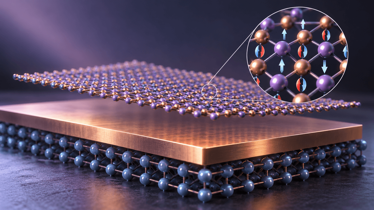
Making a promising electronic material thinner can destroy the properties that made it useful. A Brown University-led team reports a way around that problem in bismuth ferrite, preserving coupled electrical and magnetic behavior in an ultrathin film. The study appeared in Nature Materials on October 28, alongside Brown's announcement. Its significance is control of a material at dimensions relevant to devices. 1 2
In a ferroelectric material, positive and negative charge are displaced relative to each other, producing an electrical polarization whose direction can be switched. Magnetic order describes an organized arrangement of atomic magnetic moments. Bismuth ferrite is a multiferroic: it supports both kinds of order, with coupling between them. That combination creates a possible route to writing information electrically and accessing magnetic behavior, a research direction of interest for low-power memory and logic. 1
At small thicknesses, electrical and structural boundary effects can undermine that order. Brown describes two complementary remedies: a supporting crystal compresses the film through a mismatch in atomic spacing, while a conducting layer screens electric fields that would oppose its polarization. The design treats the neighboring layers as part of the material's working environment. Simply making a bulk sample smaller would not produce the same result. 1
The published abstract reports no dead layer and signatures of altermagnetism in the ultrathin limit, including a four-unit-cell structure. A unit cell is the repeating atomic building block of a crystal. Altermagnetism is a particular magnetic order in which opposing moments coexist with electronic spin behavior shaped by crystal symmetry. The authors support their interpretation with calculations, structural imaging and magnetic and photoemission measurements. The paper's careful term is “signatures,” rather than a demonstrated computing function. 2
The publication is new; the research did not first appear this week. Its arXiv record shows an initial January 15 preprint and an October 24 revision. The journal version and preprint belong to the same research program, not independent replications. The peer-reviewed publication strengthens the record for evaluating the materials result while leaving practical device performance as a further question. 3
For an electronic component, retaining useful order is necessary but insufficient. Engineers would still need to fabricate contacts, switch and read states reproducibly, characterize errors and show how the material tolerates repeated use and manufacturing conditions. An energy claim would have to include the voltages, circuitry and operations of that device. Neither a thin film nor an attractive magnetic phase establishes lower power for a complete artificial intelligence (AI) processor.
The next useful step is therefore a device-level demonstration tied to the material measurements, followed by evidence of repeatability and integration. If those stages succeed, this approach could expand the materials available for compact memory or logic. For now, the contribution is a reported route through a thickness-related failure that has obstructed that prospect, with computing applications still ahead.