Blue Light Writes Memory into Lithium Niobate
Researchers have made a light-controlled memory in a material already used for photonic chips. Oxygen implantation gives the crystal eight adjustable optical states that persist after the writing light switches off.
Published November 8, 2026Analysis / Materials / Smart Materials & Programmable Matter
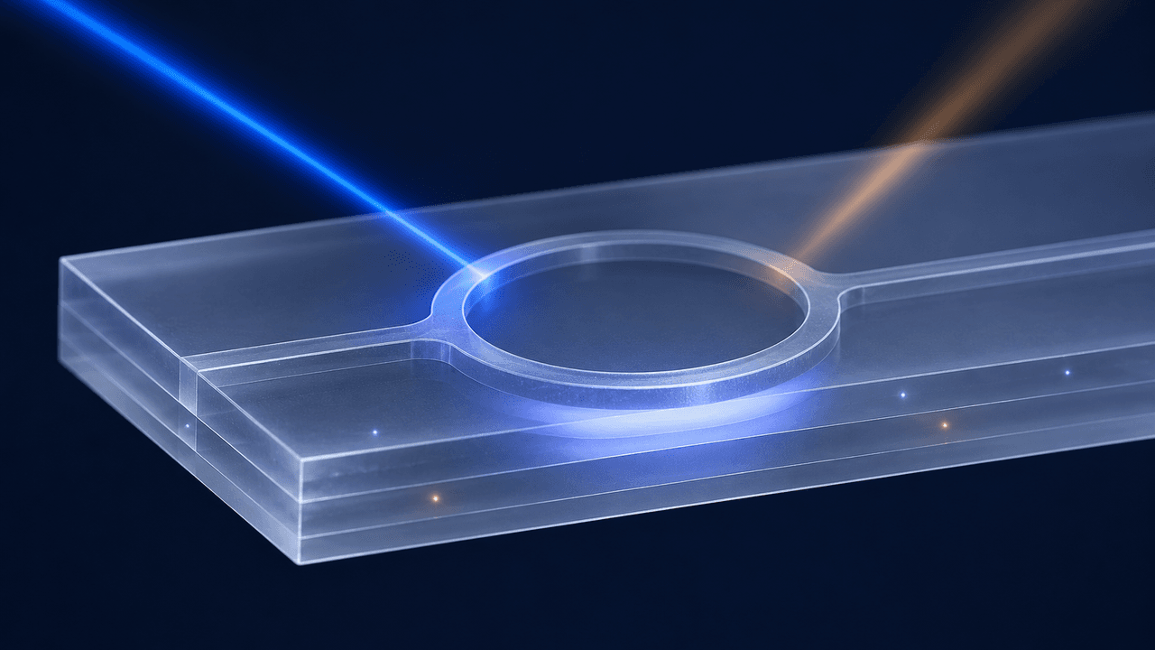
A pulse of blue light can leave a lasting setting in a tiny ring of crystal. Researchers at Shandong University in China have used that effect to create an optical memory with eight distinguishable levels. Infrared pulses move the setting back toward its starting point. Each level changes how much of a separate light signal passes through the device. [2, 3]
The work, published November 6 in Nature Photonics, addresses a practical problem in computing with light: keeping the values that tell a circuit what to do. Artificial neural networks use numerical weights to determine how strongly one signal contributes to a calculation. A photonic memory could hold such a weight where the light is being processed, allowing the circuit to reuse it. [1, 4]
Xu Gao and colleagues made the memory by implanting oxygen ions into thin-film lithium niobate, a crystal used to guide and control light on chips. The treatment allows the material itself to retain an optically written state, providing a way to incorporate memory into an established photonic platform while simplifying the task of combining different materials. [1, 2]
In one retention experiment, a written change in the device’s optical response remained nearly unchanged when checked weekly for five weeks. Between measurements, the samples were stored in darkness at room temperature and 10-15 percent relative humidity. [2]
How the crystal holds a setting
The experimental device is a microring resonator: a narrow, circular track that responds strongly to particular wavelengths of light. Changing the crystal’s refractive index, a property that governs how light travels through it, shifts those favored wavelengths. At a carefully chosen reading wavelength, that shift changes the amount of light reaching a detector. [2, 3]
Oxygen implantation gives the ring a way to retain the change. Accelerated ions enter the film, displace some atoms and eventually settle into the material. Measurements and modeling identify a defect-rich region and a deeper concentration of added oxygen. Their separation is central to the researchers’ proposed explanation. [2]
Blue light frees electrons from oxygen-related sites, the team proposes. Some become trapped at defects elsewhere in the film, leaving separated positive and negative charges. The resulting internal electric field changes the refractive index. Part of that charge separation survives after the writing pulse ends, preserving the optical setting. [2]
Infrared illumination helps the charges recombine and moves the setting back. The researchers investigated this process through spectroscopy, including measurements of changes in niobium’s electronic state, and calculations of the material’s electronic structure. [2]
The writing light had a wavelength of 450 nanometers; the erasing light was at 1,064 nanometers. A separate near-infrared beam read the result. The stored information resides in the changed material, which controls the light passing through it later. [2, 3]
Eight levels written and erased
Eight distinguishable levels correspond to three bits of information. They could also provide eight settings for an optical weight, much as a dimmer provides different brightness levels. [1-3]
To distinguish neighboring states, the researchers used a minimum spacing five times their measurement uncertainty. Each state was tested across 100 write-erase cycles. [3]
For this multilevel experiment, the team used 20-microsecond pulses, reporting 525 femtojoules for a writing pulse and 950 femtojoules for an erasing pulse. A femtojoule is a millionth of a billionth of a joule. These are optical pulse energies; a complete system would also consume electricity to produce, deliver and measure the light. [2, 3]
A separate experiment achieved controlled state changes with 800-nanosecond pulses, less than one millionth of a second. The authors’ revised experimental description, included in the public peer-review file, reports higher pulse energies for this faster operation: 850 femtojoules for writing and 1,600 femtojoules for erasing. [3]
The 800-nanosecond result provides the demonstrated benchmark for controlled memory operation. The team also investigated faster processes inside the material through spectroscopy and observed shifts in the ring’s optical response after intense femtosecond pulses. [2, 3]
Temperature tests extended the retention measurements. A device maintained two programmed settings for more than 100 hours at 55 and 85 degrees Celsius. [2, 3]
Making many memories work together
Lithium niobate has shown optical memory effects before. In January 2025, a University of Southern California team reported long-lived changes in thin-film resonators and used them to align the wavelengths at which different rings respond. The new study develops oxygen implantation as a route to reversible, multilevel memory in this material. [2, 3, 5]
The Shandong researchers also examined consistency across a newly fabricated array. In their public peer-review responses, they report testing all 280 devices under the same conditions, measuring their initial, written and erased states. [3]
Turning those devices into a computing network would require a way to select individual cells while preserving the settings of their neighbors. The supplementary information proposes separate optical control paths in a silicon-nitride layer above the lithium niobate. Simulations examine how writing and erasing light could transfer between the layers. [2]
That architecture still needs to be built and tested. Routing the control beams, stabilizing temperature and packaging the system will affect its usefulness, as will accuracy and endurance over repeated programming. [2]
The workload also matters. A photonic memory array may hold only a fraction of a large model’s weights, requiring the processor to reload them repeatedly. How often that happens, and how much energy the supporting hardware uses, will shape the value of keeping each setting in the crystal. [4]
Sources
1. Xu Gao and colleagues, “All-optical thin-film lithium niobate memristor,” Nature Photonics, November 6, 2026. Public abstract and publication record. Read source
2. Supplementary information to Gao and colleagues. Material characterization, proposed mechanism, write/erase operation, retention experiments and proposed addressing architecture. Read source
3. Public peer-review file for Gao and colleagues. Revised main-text excerpts and author responses describing 100 write-erase cycles, 800-nanosecond operation, the 280-device array and retention measurements. Read source
4. Paolo Pintus and colleagues, “Integrated non-reciprocal magneto-optics with ultra-high endurance for photonic in-memory computing,” Nature Photonics, volume 19 (2025), pages 54-62. Published online October 23, 2024. Background on retained optical weights and reprogramming overhead. Read source
5. Xinyi Ren and colleagues, “Photorefractive and pyroelectric photonic memory and long-term stability in thin-film lithium niobate microresonators,” npj Nanophotonics, January 7, 2025, updated with a publisher correction August 7, 2025. Read source